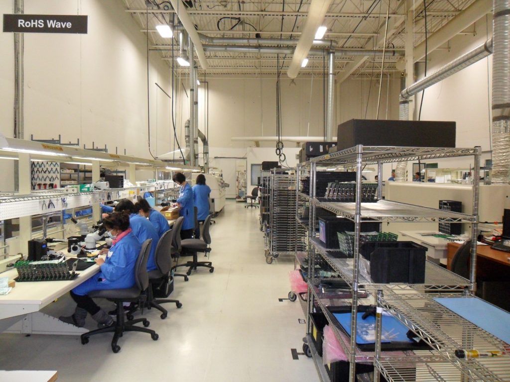
Unveiling the Intricacies of PCB Assembly: A Journey into Precision and Innovation

Printed Circuit Board PCB assembly is a critical process in the world of electronics manufacturing, playing a pivotal role in the creation of various electronic devices we rely on daily. From smartphones to medical devices, PCBs form the backbone of modern technology, connecting and powering the electronic components that make these devices function seamlessly.
Understanding PCB Assembly:
PCB assembly involves the meticulous integration of various electronic components onto a circuit board. These components may include resistors, capacitors, integrated circuits, connectors, and more. The assembly process requires precision and attention to detail to ensure that the final product meets the design specifications and functions reliably.
Key Stages in PCB Assembly:
- Design and Prototyping: The journey begins with the design of the PCB layout using specialized software. Once the design is finalized, a prototype is created to validate the functionality and identify any potential issues. This stage is crucial in ensuring that the final product meets the intended specifications.
- Component Procurement: Sourcing high-quality electronic components is a critical aspect of PCB assembly. Manufacturers must collaborate with trusted suppliers to ensure the availability of authentic and reliable components for the assembly process.
- Solder Paste Application: Solder paste is applied to the PCB to facilitate the attachment of surface-mount components. The precision application of solder paste is vital to achieving strong and reliable connections between the components and the board.
- Component Placement: Automated pick-and-place machines are employed to accurately position electronic components on the PCB. This process demands high precision to ensure that each component is correctly aligned with the design specifications.
- Reflow Soldering: The PCB undergoes reflow soldering, where it is exposed to high temperatures to melt the solder paste and create secure connections between the components and the board. Proper temperature profiles and controlled cooling are essential to prevent defects like solder bridges or cold joints.
- Quality Control and Inspection: Rigorous quality control measures are implemented to identify any defects or inconsistencies. Automated optical inspection (AOI) and X-ray inspection are common methods used to scrutinize the assembled PCB for issues such as misalignments, missing components, or soldering defects.
- Testing and Functional Verification: The assembled PCB undergoes thorough testing to ensure that it functions according to the specified parameters. Functional testing may involve checking power supply, signal integrity, and other performance metrics to guarantee the reliability of the final product.
Innovations in PCB Assembly:
Advancements in technology have led to innovations in PCB assembly, making the process more efficient and capable of handling increasingly complex designs. Some notable developments include:
- Surface Mount Technology (SMT): SMT has become the standard in PCB assembly, allowing for smaller and more densely packed components. This technology enhances the overall performance of electronic devices while reducing the size of the PCB.
- Automation and Robotics: Automated assembly systems and robotic machines have significantly increased the speed and precision of PCB assembly. This not only improves efficiency but also minimizes the risk of human error.
- Lead-Free Soldering: In response to environmental concerns, lead-free soldering has gained prominence. This approach eliminates the use of hazardous materials while maintaining the integrity and reliability of the solder joints.